Product Summary
The EP1C4F324I7N is a field programmable gate array based on a 1.5-V, 0.13-μm, all-layer copper SRAM process, with densities up to 20,060 logic elements (LEs) and up to 288 Kbits of RAM. With features like phase-locked loops (PLLs) for clocking and a dedicated double data rate (DDR) interface to meet DDR SDRAM and fast cycle RAM (FCRAM) memory requirements, the EP1C4F324I7N is a cost-effective solution for data-path applications. The EP1C4F324I7N supports various I/O standards, including LVDS at data rates up to 640 megabits per second (Mbps), and 66- and 33-MHz, 64- and 32-bit peripheral component interconnect (PCI), for interfacing with and supporting ASSP and ASIC devices.
Parametrics
EP1C4F324I7N absolute maximum ratings: (1)VCCINT, Supply voltage With respect to ground: –0.5 to 2.4 V; (2)VCCIO: –0.5 to 4.6 V; (3)VCCA, Supply voltage With respect to ground: –0.5 to 2.4 V; (4)VI,DC input voltage: –0.5 to 4.6 V; (5)IOUT, DC output current, per pin: –25 to 25 mA; (6)TSTG, Storage temperature No bias: –65 to 150℃; (7)TAMB, Ambient temperature Under bias: –65 to 135℃; (8)TJ, Junction temperature BGA packages under bias: 135℃.
Features
EP1C4F324I7N features: (1)2,910 to 20,060 LEs; (2)Up to 294,912 RAM bits (36,864 bytes); (3)Supports configuration through low-cost serial configuration device; (4)Support for LVTTL, LVCMOS, SSTL-2, and SSTL-3 I/O standards; (5)Support for 66- and 33-MHz, 64- and 32-bit PCI standard; (6)High-speed (640 Mbps) LVDS I/O support; (7)Low-speed (311 Mbps) LVDS I/O support; (8)311-Mbps RSDS I/O support; (9)Up to two PLLs per device provide clock multiplication and phase shifting; (10)Up to eight global clock lines with six clock resources available per logic array block (LAB) row; (11)Support for external memory, including DDR SDRAM (133 MHz), FCRAM, and single data rate (SDR) SDRAM; (12)Support for multiple intellectual property (IP) cores, including Altera MegaCore functions and Altera Megafunctions Partners Program (AMPPSM) megafunctions.
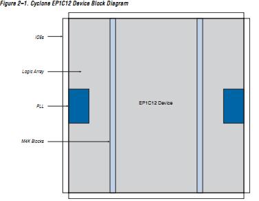
Diagrams

| Image | Part No | Mfg | Description |  |
Pricing (USD) |
Quantity | ||||||
|---|---|---|---|---|---|---|---|---|---|---|---|---|
 |
 EP1C4F324I7N |
 |
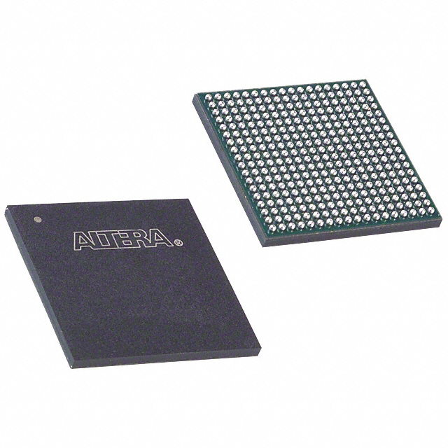
 IC CYCLONE FPGA 4K LE 324-FBGA |
 Data Sheet |

|
|
||||||
| Image | Part No | Mfg | Description |  |
Pricing (USD) |
Quantity | ||||||
 |
 EP1C12 |
 Other |
 |
 Data Sheet |
 Negotiable |
|
||||||
 |
 EP1C12F256C6 |
 |
 IC CYCLONE FPGA 12K LE 256-FBGA |
 Data Sheet |

|
|
||||||
 |
 EP1C12F256C6N |
 |
 IC CYCLONE FPGA 12K LE 256-FBGA |
 Data Sheet |

|
|
||||||
 |
 EP1C12F256C7 |
 |
 IC CYCLONE FPGA 12K LE 256-FBGA |
 Data Sheet |

|
|
||||||
 |
 EP1C12F256C7N |
 |
 IC CYCLONE FPGA 12K LE 256-FBGA |
 Data Sheet |

|
|
||||||
 |
 EP1C12F256C8 |
 |
 IC CYCLONE FPGA 12K LE 256-FBGA |
 Data Sheet |

|
|
||||||
 (China (Mainland))


